“Inside the machine that saved Moore’s Law”
(Print Title: “Inside the most complicated machine on the planet”)
MIT Technology Review, October 27, 2021
Computing
by Clive Thompson
“The Dutch firm ASML spent $9 billion and 17 years developing a way to keep making denser computer chips.”
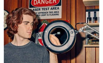
Patrick Whelan peers through the faceplate of his clean-room bunny suit to see how things are going.
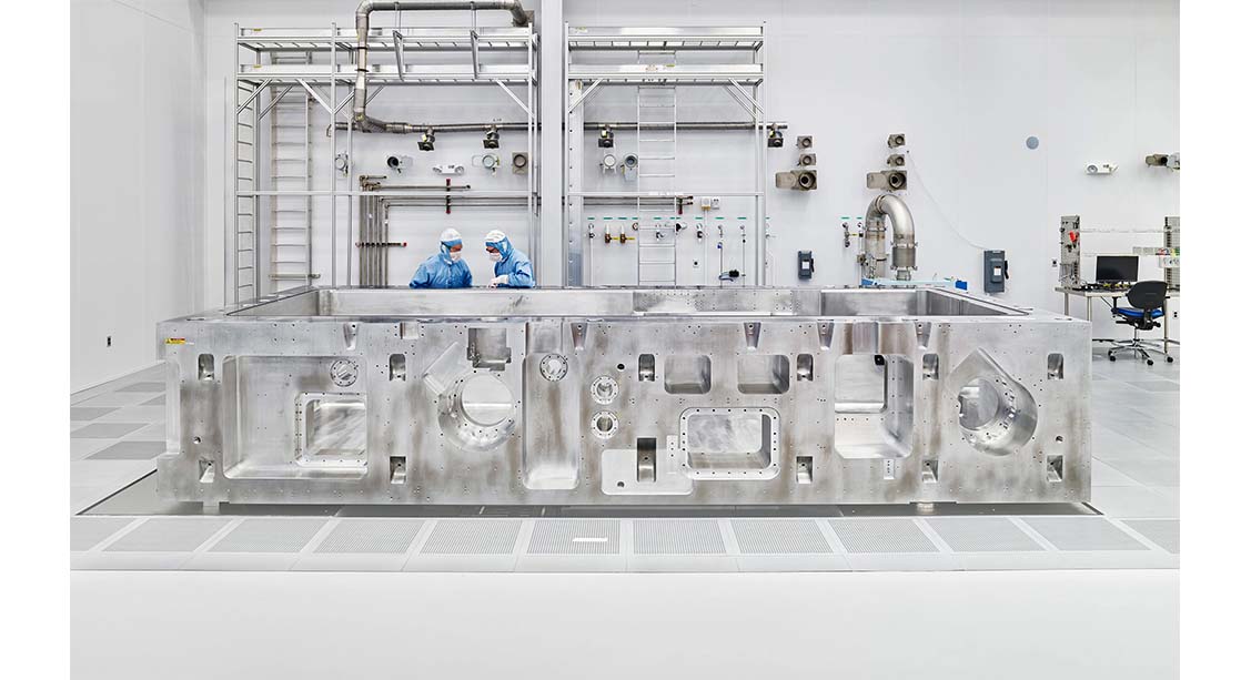
Before him is a gleaming chunk of glass, roughly the size of a toaster oven, that is carved with so many scooped-out sections to reduce its weight that it looks like an alien totem. Whelan’s team is gluing it to a large, coffee-table-size piece of aluminum. Both metal and glass are eerily smooth, having been polished for weeks to remove minute imperfections. Over the next 24 hours, as the glue solidifies, workers will neurotically monitor the position of the glass and metal to make sure they fuse together just so.
“These will be placed together to microns of precision,” Whelan tells me, gesturing at the apparatus.
A nearby technician worries he’s too close, and yelps: Back up!
“I’m not touching! I’m not touching!” Whelan says, laughing.
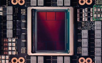
Precision is serious business here. I’m in Wilton, Connecticut, in a clean room of the Dutch company ASML, which makes the world’s most sophisticated machine for lithography—a crucial process used to create the transistors, wires, and other essential components of microchips. It’s a coveted device, with models costing as much as $180 million, that is used in making microchip features as tiny as 13 nanometers at a rapid clip. That level of precision is crucial if you’re Intel or TSMC and want to manufacture the world’s fastest cutting-edge computer processors. The final machine, assembled at ASML’s headquarters in the Netherlands, is the size of a small bus and filled with 100,000 tiny, coordinated mechanisms, including a system that generates a specific wavelength of high-energy ultraviolet light by blasting molten drops of tin with a laser 50,000 times a second. It takes four 747s to ship one to a customer.
“It’s a very difficult technology—in terms of complexity it’s probably in the Manhattan Project category,” says Sam Sivakumar, Intel’s director of lithography.
Here in Wilton, the glass-and-metal module that Whelan and his team are building is particularly critical. It will carry the patterns needed to make a microchip, and it’ll whiz back and forth while the machine blasts it with extreme ultraviolet (EUV) light, illuminating different parts of the chip pattern. The light will then bounce down to a dinner-plate-size wafer of silicon, burning the pattern in place.
Whelan walks over to a video monitor that shows one of these glass-metal contraptions zipping back and forth while being tested. It weighs 30 kilograms, but it moves in a blur.
“This is accelerating faster than a fighter jet,” Whelan says, his close-cropped beard and glasses obscured by his gear. “If there’s anything that’s loose, it’ll fly apart.” What’s more, he says, the apparatus has to stop on a spot the size of a nanometer—“so you have one of the fastest things on earth settling at pretty much the smallest spot of anything.”
This combination of speed and accuracy is key to keeping up with Moore’s Law—the observation that the number of transistors crammed into a microchip doubles roughly every two years as components become ever smaller, making the chips cheaper and more powerful. The more tightly you pack transistors, the faster electrical signals can zip around the chip. Since the ’60s, chipmakers have shrunk the components by switching, every decade or so, to a new form of light with a smaller wavelength. But by the late ’90s, manufacturers were stuck at 193-nanometer light—and they were hotly debating what to do next. The situation grew more and more dire. Chipmakers had to use increasingly complex designs and techniques to keep Moore’s Law going, but they managed to eke out another two decades of increasing performance.
Then, in 2017, ASML unveiled its production-ready EUV machine, which uses light with a wavelength of just 13.5 nanometers. With a wavelength that short, chipmakers could pack transistors more densely than ever before. CPUs can crunch numbers faster, use less power, or just get smaller. The first generations of chips with tiny EUV features are already at work for huge firms like Google and Amazon, improving language translation, search-engine results, photo recognition, and even AI that, like GPT-3, talks and writes with an eerily human quality. The EUV revolution is also reaching everyday consumers, since ASML’s machines are being used to make chips for products including some Apple smartphones and Macs, AMD processors, and Samsung’s Note10+ phone. As EUV machines become more common, it’ll boost the performance and reduce the power demands on ever more everyday devices. EUV technology also enables simpler designs, which lets chipmakers move faster and produce more chips per wafer, resulting in cost savings that can be passed on to consumers.
About the Author:
Clive Thompson is a science and technology journalist based in New York City and author of Coders: The Making of a New Tribe and the Remaking of the World.